ECE5020 Mixed-Signal VLSI Design Instructor
Steve Bibyk's Office CL381, Office Hours: Mon. & Fri: 5:15 - 6pm, Tues. 4-5pm or by email appointment. bibyk.1@osu.eduExam 1: Probably Wed. Oct. 25
Exam 2: Wed. Dec. 6, 4:10 - 5:05pm, one page of notes allowed.
Final Exam: Design Report - Softcopy in Carmen dropbox due by Dec. 11 Mon. 11:59pm
Dist Lec on Effort and Projct
ECE5020 Sheets
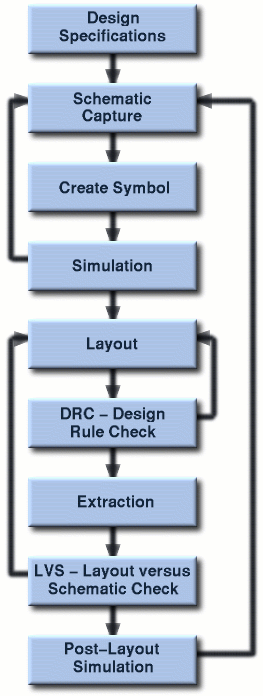
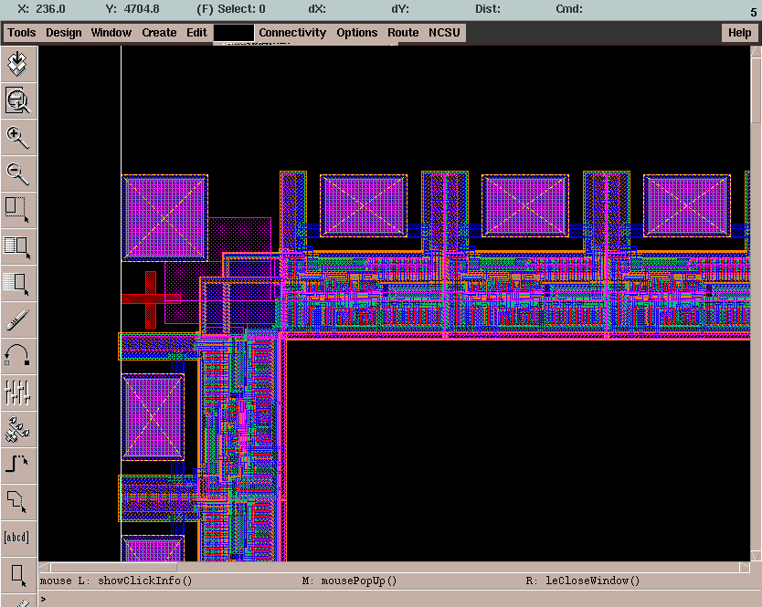
Abstracting Digital & Analog Design Flow Cadence IC Component Design Flow IC Design Project Flow System Design System Design & Language A bit slice ALU approach using programmable pass transistor function blocks Schematic, Overview, Layout , OM2 processor chip layout - left , OM2 processor chip layout - right (with ALU) ,
- Forbes Pentium 1 and Chip ASAP
- Beyond Moore's Law - Wafer Scale Integration
- FPGA/ASIC Design Process
- Manual vs. CAD Synthesis use of Standard Cell Library
- Layout with 3D Geometry
- pad frame in layout tool
- Mixed Signal System
- System Decomposition in Wireless Sensor Networks
Miscellaneous - Design and Project Guides
ECE5020 Book Links
The third edition of our textbook is a major revision, although the second edition is fine to use.
Some of the new chapters are online at: Weste and Harris, 3rd ed.
Plenty of course material and many useful links from Prof. D. Harris' web site are online at: Author's course website
from 2nd ed. ece5020 textbookThe next book site is for a textbook we could switch to someday, it also has a large amount of online content.
Digital ICs by J. Rabaey et al It's the textbook used at the Univ. of Virginia site below.
Here are some pertinent comments in the 1st edition Preface Top Down vs. Bottom Up
Here are a few key slides from his Chp. 1 ppt slides (online) Intro Chapter pointsIntel Research Technology.
Find the VLSI Circuit ones, such as in the Microprocessors and Silicon Areas. Intel Silicon Technology.
Project CAD Tools
Setup Cadence See Cadence Tool setup, NCSU ver 1.2. Note item 5, the upgrades to the Mentor Graphics link.
You will need CAD tools for the project. For tutorials on how to use Cadence, see the section on Tutorials on the Setup webpage.
A specific tutorial from SJSU on custom digital IC project for telephony is given here SJSU IC Engineer TutorialThe Cadence tools have a huge set of help files ( > 177MB ) which can be accessed either within tools or directly in the doc directory
(eg. /opt/local/cadence/IC5033/doc...). Here is an example helpfile file for Virtuoso Composer Schematic entry: Schematic EntryVarious CAD tools are listed at the following MOSIS link. Electric is free and a decent overall package.
Full Custom CAD tools
Another free sent of tools for large digital ASIC design flows is at: Alliance tools
One of the main difficulties with CAD tools, especially free ones, are the lack of design kits and libraries
for MOSIS type IC fabrication processes. That's one of the reasons we use a Cadence design flow.Univ. of Virginia (Prof. Mircea Stan) - Cadence Tutorials
Using Cadence for Project work
CAD tool use for chip design
One goal of the project work is to get familiar with design flows for chip design. In design, it is helpful to know how
to interact with the chip fabrication and testing companies.A good source for how to deal with chip fabrication companies (foundries) is at: Mosis Chip fabrication broker
The content at this link shows the scope of know-how that is needed: Mosis Support by TopicA more open information broker is Circuits Mulit-Projects (CMP) in France: CMP
Here are some classic cell libraries for chip design for our study.
AMI 0.5um Padframe Library , AMI 0.5um Design Library
PROJECT INFORMATION
Link to Asynchronous Digital Design Course ModulesAutomating Digital Design in Mixed Signal Systems James Copus' Digital Synthesis Thesis
Project Topics are discussed in Class. Here is a partial list of Project Options:
An example topics from the past is: Asynchronous Logic Circuits
An example final report from last time is: Past Report on Wavelet ASIC Note the tips in the conclusion.
Here is a MidWest Circuits Conference paper that came from an ECE 5020 project. EEProm Conference Paper , Midwest Circuits & System Conference
Here is a paper that came from OSU VLSI chip design research. Vampire Video Chip Paper
Here is a nice link to memory design considerations CMU memory course , Memory Compiler Tutorial